New laser material processing patents significantly increase SiC productivity
Abstract Scientists at DISCO Japan use a patent called patent-named key-amorphous-blackrepetitive absorption (KABRA) and patent-pending...
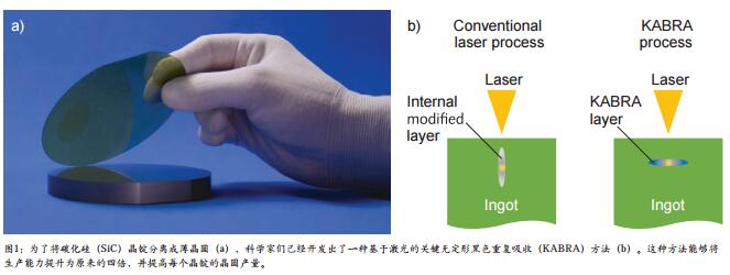
Scientists at Japan's DISCO use a patent called key amorphous-black repetitive absorption (KABRA) and patent-pending laser material processing technology to increase the productivity of silicon carbide (SiC) wafers. Increased to four times the original and reduced material loss while increasing production. This technique is applicable to single crystals and polycrystalline ingots regardless of the orientation of the crystal layer. At present, the penetration of SiC power devices in the market is slow, mainly because of its small output and high production cost. However, the KABRA method can significantly increase the yield of SiC devices and should enable SiC devices to gain more market-driven power as products such as power devices, space mirrors, ultra-stable optical molds, and bolometers. In order to produce SiC wafers with a thickness of 350 μm using a 20 mm thick ingot with a diameter of 4 inches, the traditional diamond wire saw process requires 1.6 to 2.4 hours to cut each wafer, followed by double side grinding. The process and final polishing process, which produces 30 wafers from an ingot, takes a total of 2.5 to 3.5 days. Although many polishing processes are under development, SiC is still a very hard and brittle material, and SiC must be ground very carefully due to the formation of deep undulating grooves during mechanical cutting.

KABRA wafer separation
As can be seen from its name, the KABRA process essentially focuses the laser inside the SiC wafer, decomposing SiC into amorphous silicon and amorphous carbon by repeated pass or "amorphous black repeat absorption" and forming it as a wafer. A layer that separates the base points, that is, the black amorphous layer absorbs more light, so that the wafer can be easily separated (see Figure 1). Compared to 1.6 to 2.4 hours in the conventional process, the KABRA process separates each wafer in only 25 minutes, compared to the use of conventional slicing processes, which result in a material loss of 200 μm per wafer, during the separation of the KABRA process. No material loss occurs. In addition, wafer saw-separated wafers require 16 hours of final grinding time, which is not required in the KABRA process.
In short, using traditional processes, it takes 2.5 to 3.5 days to produce 30 wafers from an ingot. Using the KABRA process, 44 wafers are produced from an ingot, which takes only 18 hours. This is equivalent to a 3 to 5 times productivity increase (or about four times the capacity).
Let Street Light,Spot Lights Outdoor,Outdoor Garden Lighting,Waterproof Led Light
JIANGMEN MICHEN LIGHTING CO.,LTD , https://www.jmledbulb.com